Skip to:

MRFN Member Login
Program Application

The Nanoscale Imaging and Analysis Center (NIAC) at the University of Wisconsin-Madison

The central NIAC facility has provided materials researchers and industrial clients with electron microscopy imaging and analytical analysis, surface analysis and x-ray diffraction serves for over 25 years. The NIAC houses:
 

  • Dynacool PPMS System
  • J.A. Woollam Variable Angle Spectroscopic Ellipsometer (VASE) and Infrared VASE (IR-VASE) systems
  • Cameca Local Electrode Atom Probe
  • Three scanning electron microscopes with Electron Dispersive X-ray spectrometers
  • Four transmission electron microscopes, with Cryo TEM tomography and an FEI Titan aberration corrected (S)TEM
  • A surface analysis instrument: a Thermo Fisher k-alpha X-Ray Photoelectron Spectrometer
  • Three atomic force microscopes including a Bruker Icon and a Bruker Catalyst BioAFM
  • Two dual-beam focused ion beam instruments, including a Plasma Focused Ion Beam
  • An Andor Spinning Disk Confocal Microscope
  • A confocal micro-Raman spectrometer (Horiba LabRAM HR Evolution)
  • A small-angle x-ray diffractometer (SAXS)
  • Three additional Diffractometers
  • A ZYGO Optical Interferometer
  • A Horiba Nanolog spectrofluorometer
  • A UV/VIS Dual Beam Fluorometer

For use, questions or more information, please contact the DIrector of MRSEC facilities:

Dr. Jerry Hunter

(608) 263-1073

jerry.hunter@wisc.edu


Instruments

  1. Andor Spinning Disk Confocal Microscope

    The Andor spinning disk confocal is an optical imaging technique with increased resolution as compared to widefield microscopy. Higher scanning speeds are possible with spinning disk confocal, decreasing the potential for sample photobleaching and phototoxicity.

  2. Bruker Bioscope Catalyst Atomic Force Microscope (AFM, Bio-AFM, Scanning Probe Microscope (SPM))

    Bruker's latest innovations, including Peak Force Tapping and the new Nanomechanics Package, significantly expands BioAFM applications in mechanobiology research and expands support for a lower modulus range covering live cells and tissues. With its open-access design, integrated software for combined AFM and fluorescence imaging, along with the bio-friendly features and accessories, the Bioscope Catalyst is the most integrated and easiest to use life science AFM available.

  3. Bruker D8 Discover Diffractometer X-Ray Diffractometer (XRD)

    Synopsis:
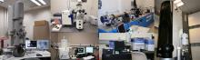
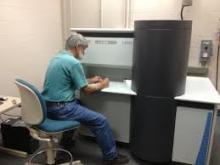
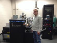
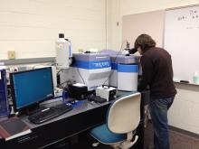
    The Bruker D8 Discover diffractometer is ideally suited for rapid phase identification, stress analysis, and texture determination. It also has mapping capabilities with ~0.1 mm lateral resolution and can be configured for small angle x-ray scattering (SAX).

    Advanced X-ray Diffraction System for Materials Research Applications

  4. Bruker Icon AFM

    The Icon AFM incorporates the latest evolution of Bruker’s industry-leading nanoscale imaging and characterization technologies on a large sample tip-scanning AFM platform. The Icon’s temperature-compensating position sensors render noise levels in the sub-angstroms range for the Z-axis, and angstroms in X-Y.

    The Icon AFM in the NIAC allows has Peak Force Tapping, the Quantitative Nanomechanical Analysis software and the Fast Tapping as available options.


  5. Bruker Multimode 8 Atomic Force Microscope (AFM, SPM)

    The MultiMode AFM offers multiple SPM modes, including contact AFM, TappingMode and Peak Force Tapping.

  6. Cameca (Imago) Local Electrode Atom Probe (LEAP)

    The LEAP Si is a high performance atom probe microscope which provides nano-scale surface, bulk and interfacial materials analysis of simple and complex structures with atom-by-atom identification and accurate spatial positioning.
    The system works using the principle of field evaporation, whereby a strong electric field applied to the specimen is sufficient to cause removal of atoms by ionization. Atom removal is triggered either via a voltage or laser pulse applied to the sample.

  7. Cameca IMS-4fE7 Secondary Ion Mass Spectrometer

    The Cameca 4f-E7 provides depth profile and contamination analysis on a broad range of materials from semiconductors and metals to insulators.

    It is equipped with oxygen and cesium primary ion sources for analysis of positive and negative secondary ions and a high resolution (30,000 m/dm) double focussing mass spectrometer.

  8. CryoUltraMicrotome

    The Ultramicrotome Leica EM UC7 provides easy preparation of semi- and ultrathin sections as well as perfect, smooth surfaces of biological and industrial samples for TEM, SEM, AFM and LM examination. Equipped with EM FC7 cryo option.

  9. Dynacool PPMS

    The Dynacool PPMS has recently been installed at the UW Madison Nanoscale Imaging and Analysis Center. 

  10. FEI Titan Aberration-corrected (S)TEM

    This FEI STEM instrument is configured with a CEOS probe-side aberration corrector, which provides revolutionary performance in STEM imaging and microanalysis. Imaging single atoms, and nanoscale Chemical and Structure analysis. With <0.08 nm spatial resolution Zcontrast STEM imaging, <0.1 nm spatial resolution HRTEM imaging. It is fully equipped for analytical analysis with EDS and electron energy loss spectrometers.

  11. FEI Vitrobot

    Plunge Feeze CEVS system automadited to prepare vitrified TEM sections of aqueous samples, biological or polymer thin sections.

  12. Horiba LabRAM HR Evolution Raman Spectrometer

    The LabRAM HR Evolution Confocal Raman Microscope provides measurements of spectra and 2-d mapping of true confocal Raman and photoluminescence in the range from near- IR to UV. The instrument contains 4 excitation sources and has fast mapping mode.

  13. Hysitron TI950 Triboindenter

    The TI 950 TriboIndenter nanoindenter has been developed as an automated, high throughput instrument to support the numerous nanomechanical and nanotribological characterization techniques developed by Hysitron. Transducers available for the TI 950 include scratch, dynamic mechanical analysis (DMA), high load (to 10 N), acoustic emission, conductive probe and Xprobe, allowing for a wide range of testing methods.

  14. Leica EM TiC 3X Ion Beam Milling System

    The Wisconsin Centers for Nanoscale Technology installed a Leica EM TiC 3X Ion Beam milling system. Funding was provided by the UW-Madison MRSEC, COE, L&S, VCRGE and CALS. The system is currently available for use in the Nanoscale Imaging and Analysis Center.

    Features

  15. Malvern PANalytical X'Pert PRO X-Ray Diffractometer (XRD)

    High Resolution XRD for Rocking curves and Reciprocal space maps.Six-axis sample stage on high resolution goniometer. Absolute angular resolution = 0.0001 degrees.

  16. Micro FT-IR Spectrometer

    Thermo Nicolet Magna 550 FT-IR bench with a NICPLAN FT-IR Microscope with computer controlled Stage. Latest Omnic/Atlas software for spectral mapping of areas by stage scanning. Bulk and Micro FT-IR measurements on a variety of samples.

  17. NanoMill

    The NanoMill system features gaseous ion source technology that results in ion energies as low as 50eV and a beam size as small as 2 microns. It allows specimens to be prepared without amorphization, implantation, or re-deposition. The ion beam can be targeted to a specific area of interest. A secondary electron detector (SED) is used to image the ion-induced secondary electrons that are generated from the targeted area of the specimen.

  18. PANalytical Empyrean X-ray diffractometer

    Area detector for high speed, high sensitivity and 2D X-ray diffraction data collection


  19. Small-angle X-ray Scattering System XRD

    SAXS with micro focus Cu sealed tube. With cross coupled multilayer mirrors operates at 40 W.and 20 um by 20 um source size. Automatic multiple sample scanning capability and Heating and cooling: Linkam temperature stage. A liquid cell is available.Sample to detector length: 2 meters. Detector is 2-dimensional multi-wire with 1024 by 1024 wires over a 6-inch area

  20. Tecnai Cryo Transmission Electronc Microscope (TEM)

    A state of the art Technai T12 transmission electron microscope with high quality digital imaging capabilities. The electron microscope is the standard for sub-cellular ultrastructural imaging at high magnification. Equipped for cryoTEM.

  21. Tecnai TF-30 300KV Field Emission Scanning Transmission Electron Microscope (FE STEM)

    This 300 KV STEM is equipped with a Field Emmison source, and equiped for cyro samples, and normal hard materials work. With an automated stage and tilt of +70 to -70 degrees it is capable of electron tomography including various software pacjages. Double tilt holder allows easy diffraction work for multiple zone axis while the samples is in the microscope. HigH resolution CCD as well as side entry fast cameras, and Gatan GIF.

    Features & Accessories:

  22. ThermoFisher Helios G4 UX Plasma Focused Ion Beam/Field Emission Scanning Electron Microscope

    The Helios Plasma Focused Ion Beam (PFIB) Workstation is a fully digital, Extreme High Resolution (XHR) Field Emission Scanning Electron Microscope (FE SEM) equipped with inductively coupled plasma (ICP) focused ion beam (PFIB). It allows in-situ large area sample preparation and high resolution imaging and analysis of
    hundreds of microns areas.

  23. Wisconsin MRSEC X-ray Endstation for Nanoscale Transformations (MXNT)

    The Wisconsin MRSEC has developed a versatile synchrotron-radiation instrument enabling the use of hard x-ray nanobeam and coherent scattering techniques to study nanoscale phenomena in the formation, crystallization, and transformation of nanoscale volumes of materials in carefully controlled environments. The instrument is specifically designed to permit the use of close-working-distance x-ray optics using either Fresnel zone plates (for experiments with photon energies from 5 to 12 keV) or compound refractive lenses (from 12 to approximately 25 keV).

  24. X-ray Photoelectron Spectrometer (XPS)

    The Thermo Scientific™ K-Alpha™+ X-ray Photoelectron Spectrometer (XPS) System is a fully integrated, monochromated small-spot XPS system with depth profiling capabilities. State-of-the-art performance, reduced cost of ownership, increased ease of use and compact size make the K-Alpha X-ray XPS System ideal for a multi-user environment.

  25. Zeiss Auriga Focused Ion Beam FIB/FESEM

    The Zeiss Auriga SEM combines SEM imaging with FIB capabilities. The live SEM imaging capability during FIB operation mode gives full control when micro-machining critical samples.

    The Auriga series offers a multi-channel gas injection system for ion beam deposition of metals or insulators and for enhanced etching. A wealth of options exist on the NIAC system including a 5 gas injection system and a single high angle gas injector for 0 degree, an in situ micromanipulator, and SE, Inlens SE, Inlens BSE, STEM and EDS detectors.

  26. Zeiss Gemini 450 FESEM

    The Zeiss GeminiSEM 450 is a high-performance variable pressure Scanning Electron Microscope (SEM) equipped with a Schottky type field emission gun, various detectors (in-lens and Everhart-Thornley type secondary electron detectors, as well as a variable pressure secondary electron detector, an in-lens back scattered electron detector, and multi-quadrant solid state back-scattered electron detector). In addition, there is a detector for energy-dispersive x-ray analysis. This system has an oil free vacuum system to maintain hydrocarbon free imaging.

  27. Zeiss Leo 1530 FESEM/EDS/EBSD

    The LEO 1530 uses a Schottky-type field-emission electron source. The Gemini optical column has no crossovers and utilizes a magnetic/electrostatic objective lens for outstanding imaging capabilities, especially at low voltage (due to reduced chromatic aberration.EDS with SSD detector. Large area fast BSE detector.

  28. ZYGO 9000 Optical Profilometer

    The ZYGO white light interferometer (profilometer) is a tool for characterizing and quantifying surface roughness, step heights, critical dimensions, and other topographical features with excellent precision and accuracy. All measurements are nondestructive, fast, and require little to no sample preparation. Profile heights ranging from < 1 nm up to 20000 nm at high speeds, independent of surface texture, magnification, or feature height!